Science & Technology

MoD signs three contracts worth ₹5,400 crore

Context: Ministry of Defence (MoD) has signed three contracts worth ₹5,400 crores recently. All these projects are under Buy {Indian – IDMM (Indigenously Designed Developed and Manufactured)} category.

Major Highlights

  • Two contracts were signed with Bharat Electronics Limited (BEL) worth ₹2,400 crores for the procurement of:
    • Automated Air Defence Control and Reporting System ‘Project Akashteer’ for the Army
    • Sarang Electronic Support Measure (ESM) systems for the Navy.
  • Another ₹2,963 crore contract was signed with NewSpace India Limited (NSIL) for an advanced communication satellite, GSAT 7B, for the Army. 

Project Akashteer

  • ‘Project Akashteer’ worth ₹1,982 crores is an automated air defence control and reporting system that will allow the army’s air defence units to operate in an integrated manner.
  • It will enable monitoring of low-level airspace over the battle areas of the Indian Army and effectively control the ground-based air defence weapon systems.

Sarang Electronic Support Measure (ESM) systems

  • The second contract worth ₹412 crores with BEL is for Sarang Electronic Support Measure systems for Indian Navy helicopters. ‘Sarang’ is designed and developed indigenously by the Defence Electronics Research Laboratory, Hyderabad under the programme, Samudrika.
  • It will generate employment of approximately two lakh man-days over a period of three years.

GSAT 7B

  • The five-tonne geostationary satellite will be developed indigenously by Indian Space Research Organisation (ISRO).
  • The satellite will considerably enhance the communication capability of the Indian Army by providing mission-critical beyond-line-of-sight communication to troops and formations as well as weapon and airborne platforms.
  • The Army is likely to get the satellite in 2026. Unlike the Indian Air Force and the Navy, the Army currently does not have a dedicated satellite.

Many parts and sub-assemblies and systems of the satellite will be sourced from indigenous manufacturers, including micro, small and medium enterprises (MSMEs) and start-ups. The project will generate employment of around 300,000 man-days over the next three-and-a-half years.

Massive coronal hole found on sun, it's 20 times larger than Earth: Experts

Context: The sun has developed a massive “hole” 20 times larger than Earth, marking the second such occurrence in a week. The coronal hole is unleashing solar winds of 2.9 million km/h toward Earth. 

More on the news: Scientists are carefully monitoring the situation to assess if the winds will impact our planet’s magnetic field and satellites – with the potential for knock-on effects on the internet, mobile phone networks, and GPS. It is also noteworthy to scientists as it has appeared near the sun’s equator. NASA’s Solar Dynamics Observatory captured holes.

Coronal holes

  • Coronal holes are areas of the Sun's corona where the magnetic field is open and allows for the escape of high-speed solar wind particles. 
  • Coronal holes are usually harmless, experts say and are usually found near the sun’s poles.
  • These areas appear as dark regions in images of the Sun's corona taken in ultraviolet and X-ray wavelengths. 
  • Coronal holes are characterized by low magnetic field strength and low temperatures compared to the surrounding areas.
  • Coronal holes are thought to be related to the Sun's magnetic field and the Sun's 11-year solar cycle, with more coronal holes appearing during times of high solar activity.
  • They are cooler, less dense areas of the star and appear during the less active stage of the sun’s 11-year cycle.
  • Coronal holes are magnetically open areas that are one source of the high-speed solar wind.
  • At times, the solar wind can generate aurora at higher latitudes on Earth. That coronal hole produced auroras far further south than usual, with the skies over Arizona turning an electric purple and green.
  • The solar wind particles that escape from coronal holes can impact Earth's magnetic field, causing auroras and other geomagnetic disturbances. Scientists study coronal holes to better understand the Sun's magnetic field and its effects on the space environment around Earth.

SOLAR ENERGETIC PARTICLES (SEP), SOLAR WINDS AND FLARES, AND CORONAL MASS EJECTIONS (CMES)

Solar flares and Coronal Mass Ejections (CMEs)

  • CMEs and Solar flares are both explosions that occur on the sun. Sometimes they occur together, but they are not the same thing - they emit different things, they look and travel differently, and they have different effects near planets.
  • Both eruptions are created when the motion of the sun’s interior contorts its own magnetic fields. Both originate from corona. 
  • Solar flares are giant burst of X-rays and energy which travel at the speed of light in all directions. 
  • CME are giant cloud of particles (mostly protons and electrons and powerful magnetic fields) hurled into the space, in particular direction. CMEs take one to three days to reach the earth. Flares only takes eight minutes. 
  • Flares and CMEs have different effects at Earth as well. The energy from a flare can disrupt the area of the atmosphere through which radio waves travel. This can lead to degradation and, at worst, temporary blackouts in navigation and communications signals. On the other hand, CMEs can funnel particles into near-Earth space. A CME can jostle Earth’s magnetic fields creating currents that drive particles down toward Earth's poles. When these react with oxygen and nitrogen, they help create the aurora, also known as the Northern and Southern Lights.
  • A solar flare is a sudden flash of increased brightness on the Sun, usually observed near its surface and in close proximity to a sunspot group. Powerful flares are often, but not always, accompanied by a coronal mass ejection. 
  • Solar flares affect all layers of the solar atmosphere (photosphere, chromosphere, and corona).
  • Flares occur in active regions around sunspots, where intense magnetic fields penetrate the photosphere to link the corona to the solar interior.
  • Flares are powered by the sudden release of magnetic energy stored in the corona.

Solar winds constantly occur due to the corona of the sun continually expanding. The solar wind is a stream of charged particles consisting of electrons, protons and alpha particles with kinetic energy between 0.5 and 10 keV. The composition of the solar wind plasma also includes a mixture of materials found in the solar plasma: trace amounts of heavy ions and atomic nuclei C, N, O, Ne, Mg, Si, S, and Fe.

Solar energetic particles (SEP) 

  • They are high-energy particles coming from the Sun. 
  • They were first observed in the early 1940s. 
  • They consist of protons, electrons and high-energy nuclei with energy ranging from a few tens of keV to many GeV. 
  • They are of particular interest and importance because they can endanger life in outer space (especially particles above 40 MeV). But their onset is extraordinarily hard to predict, in part because we still don’t know exactly where on the Sun they come from.
  • The greatest mystery about gradual SEPs is not what speeds them up, but where they come from in the first place. For reasons still not fully understood, SEPs contain a different mix of particles than the other solar material streaming off the Sun in the solar wind – fewer carbon, sulfur, and phosphorous ions, for instance. 
  • Many scientists thought Solar Energetic Particles would be found at the edges of the active region where the magnetic field is already open and material can escape directly. But the fingerprint matched only in regions where the magnetic field is still closed.
  • The SEPs had somehow broken free from strong magnetic loops connected to the Sun at both ends. These loops trap material near the top of the chromosphere, one layer below where solar flares and coronal mass ejections erupt.

Indian Biological Data Centre (IBDC)

Indian Biological Data Centre is India’s first national repository of life science data at Faridabad, Haryana at the Regional Centre of Biotechnology.

What is IBDC?

It will archive all life-science data generated from publicly funded research in India without any infringement on intellectual property. Intellectual property of the data remains solely with the owner of data.

  • IBDC has a data storage capacity of about 4-petabytes and houses the Brahm – High Performance Computing facility. 
  • The repository is being funded by Department of Biotechnology, under Ministry of Science & Technology.
  • Data on the nucleotide data, protein data, human genome, crop genome, RNA, medical imaging, disease and surveillance data would be stored in the unique facility. 
  • It has accumulated over 200 billion bases from over two lakh submissions from more than 50 research labs across India. 
  • IBDC is being developed in a modular fashion wherein different sections would typically deal with particular type/s of life science data.

indian biological data centre has started data submission services via two data portals:

  1. Indian Nucleotide Data Archive (INDA): Data shared with this portal is actively synced with International Nucleotide Sequence Database Collaboration and is simultaneously assigned IDs from both IBDC and INSDC repositories. 
  2. Indian Nucleotide Data Archive – Controlled Access (INDA-CA): Data shared with this is not shared with any international repositories and remains under ‘controlled access’ as per the user requirements. Users would decide who can access the data. 

Users are free to submit data to any of these repositories as their needs.

International Nucleotide Sequence Database Collaboration (INSDC)

  • INSDC is the core infrastructure for sharing nucleotide sequence data and their subsidiary information called metadata in the public domain. 
  • The collaboration is comprised of three nodes that keep the identical information through a daily data exchange process that has operated over 30 years. 
  • INSDC provides uniform policy of free & unrestricted access to all of data records their databases contain, with no restrictions on access, redistribution or republication of data. 

Members of INSDC

  1. DNA Data Bank of  Japan (DDBJ) at National Institute of Genetics in Mishima, Japan.
  2. European Nucleotide Archive (ENA) at the European Molecular Biology Laboratory’s European Bioinformatics Institute (EMBL-EBI) in UK. 
  3. GenBank at National Centre for Biotechnology Information (NCBI).

Quantum Communication

Context: At the first International Quantum Communications Conclave in New Delhi in March 2023, it was announced that India’s first quantum computing-based telecom network link is operational. 

  • The secure line is between Sanchar Bhawan and the National Informatics Centre at the Central Government Offices (CGO) complex in Delhi.

Quantum communication 

  • Quantum communication is an amalgamation of quantum mechanics and modern communication and Information Technology to study data transmission and processing. It takes advantage of the laws of quantum physics to protect data and securely transmit data.
  • Conventionally, sensitive data is encrypted and sent through fibre optic cables with a digital “key” to decrypt the information. This data is transmitted in classical binary bits (0s and 1s), which makes it vulnerable to hackers who can read and copy it without a trace. Theoretically, this makes these networks ultrasecure. 
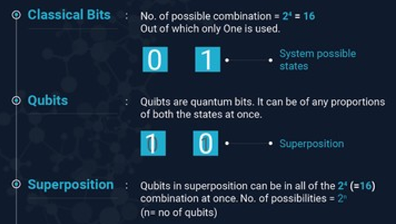
  • However, in a quantum communication network, data is transmitted via quantum bits or qubits. Qubits are particles, usually photons of light, in a superposition state, i.e., they can be in multiple states and represent numerous combinations of 0 and 1. If a hacker tries to read this data, the qubits would “collapse” from their fragile quantum state to either a 0 or 1, thereby leaving a clear trace of external activity. 
k o7Ij72w0o3wiY1NXNpYgNVZTZhRO3xhGN 5X3EyDo5x6nFBkKBue18iI7imgruNspg9YW8KpzNd8WxcO5BIzJF8Zy8VysTV EUxRpd6qEQ4uBXXQciQwadLx 15dLfiFLgIYVsVvEJpF3VkAsPfA

Data encryption in a quantum communication network

  • Companies have recognised the additional security offered by quantum communication networks and have taken to transmitting sensitive data through a process called quantum key distribution (QKD).
    • QKD involves the transmission of encrypted data as classical bits over networks while the decryption key is encoded and transmitted in a quantum state using qubits.
    • The most widely used scheme for this is the BB84, the world’s first quantum cryptography protocol.

Concerns

  • Theoretically, Quantum Communication networks are highly secure, with the built-in security of qubits and the simplified traceability of external interference in the signal. However, these are predicated on the assumption that the machines used in the data encryption and transmission are secure and perfect, which may not be the case.
  • The decay of the signal due to decoherence and the need for quantum repeaters for long-distance transmission is a systemic vulnerability that needs to be addressed.
    • Quantum repeaters are nodes where the quantum keys are decrypted into bits and re-encrypted in a fresh quantum state to avoid signal loss. 

Bio-Bitumen

Context: As per the Ministry of Road and Highways, making bitumen from agricultural waste such as rice husk can help save up to ₹30,000 crores annually in import bills.

Major Highlights

  • India requires around 80 lakh tonnes of bitumen annually for roads. Of this, around 50 lakh tonnes are provided by domestic refineries for processing crude oil, and around 25-30 lakh tonnes are imported costing around 25,000-30,000 crore.  
  • Recently, the Council of Scientific and Industrial Research (CSIR) and the Central Road Research Institute (CRRI) have developed technology to make bitumen from rice husk, which is supposed to be better than bitumen extracted from crude oil.
    • This makes 70% bitumen and the rest is biochar or organic carbon. Organic char can enhance farm productivity. 
  • The Ministry envisions opening up to 1,000 such units in rural India to produce bio-bitumen and completely do away with the burning of husk or agri-waste which leads to pollution. It would benefit the farmers in states such as Delhi, Punjab, Haryana and Uttar Pradesh.
SeEcGrM1Hxl0YeGTJQPh6DqaOJPpqelH32rAsQTBCBn1Pk

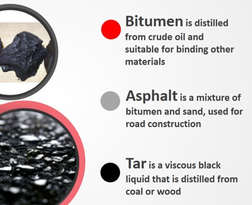
Bitumen

  • Bitumen is a dense, highly viscous, petroleum-based hydrocarbon produced during the refining process or distillation of crude oil. Bitumen is known for its waterproofing and adhesive properties and is commonly used in the construction industry, notably for making roads and highways. 

Bio-bitumen would play a significant role as a road construction material to replace the fossil-based version while curbing CO2 emissions and boosting the bio-economy.

Nitrosamines

Context: European Food Safety Agency has recently warned that cancer-causing chemical compounds called nitrosamines have been detected in various everyday foods and could pose a health risk to consumers.

  • Nitrosamines are a class of chemical compounds that are known to be potentially carcinogenic (cancer-causing) to humans. They are formed when nitrites and amines, which are commonly found in many food and beverage products, react with each other under certain conditions, such as high temperatures or acidic environments.
  • Nitrosamines have been detected in cured meat, processed fish, cocoa, beer, and other alcoholic drinks.
  • Meat is the most important food group contributing to nitrosamine exposure.
  • Exposure to nitrosamines has been linked to an increased risk of various types of cancer, including stomach, colon, and pancreatic cancer. They can also have other adverse effects on health, including liver damage, respiratory problems, and reproductive toxicity.
  • To reduce the risk of exposure to nitrosamines, it is recommended to limit consumption of processed meat and other foods that contain nitrites, as well as to ensure proper storage and preparation of these products. Additionally, individuals can choose to consume organic and nitrate-free food products to further minimize exposure to nitrosamines.

Gravity Based Batteries in Kolar Gold Field

Context - An Australian renewable energy company’s unique Scheme to generate electricity may resuscitate the fortunes of one of India’s iconic but defunct gold mines, namely the Kolar Gold Fields (KGF), in Karnataka.

How do Gravity Batteries work?

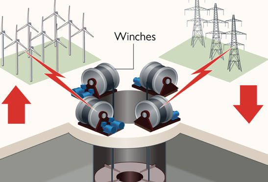
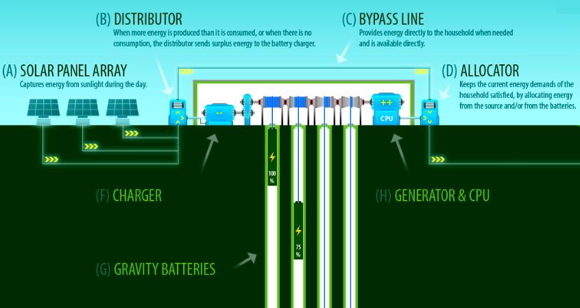
  • When there is plenty of green energy, the batteries use the power to lift a heavy weight either high into the air or to the top of a deep shaft.
  • Then when the renewables are limited, winches gradually lower the weight, release the load, powering a generator with the downward gravitational pull from the movement of the cables.
  • This would mean you could store power captured by a solar farm during the day when the sun is shining, and then release that electricity to the grid in the evening when demand rises because people are at home using electricity to watch TV, cook and heat their homes.
Diagram

Description automatically generated
Diagram

Description automatically generated with low confidence

Gravity batteries vs Lithium-ion

Gravity batteries are not the only way renewable energy can be stored, lithium-ion batteries dominate the market, and some experts favour green hydrogen. But gravity is free, clean and easily accessible, without the complications of producing hydrogen or the environmental and human rights concerns linked to some lithium mining.

Storing power in mineshafts

Full-scale energy stores in former mines can make good use of existing infrastructure and create jobs in exactly those areas where they’re most needed. The emotional aspect of this is also important. Whole communities once worked in the mines - and generally, they’re very happy to see them used for storing renewable energy.”

Note - The World Economic Forum founded the Global Battery Alliance (GBA) in 2017 to establish a sustainable battery supply chain by 2030. The body of over 100 leading international organizations, NGOs, industry actors, academics and multiple governments became independent in 2021 and its membership is collectively working towards the goals set out in the GBA 2030 Vision. The GBA 2030 Vision is to foster a circular, responsible and just battery value chain.

The GBA hosts Action Partnerships to achieve its vision of a sustainable battery value chain by 2030, including:

The Battery Passport Action Partnership: to establish global criteria, data and benchmarks for a sustainable and transparent battery market;

Critical Materials: to ensure critical materials are sourced, processed, manufactured and recycled in a manner that minimizes environmental impacts, protects human rights and creates benefits for stakeholders along the value chain.  

Energy Access & Circularity: to ensure energy access in emerging economies, reduce lead poisoning and promote circularity.

Biotransformation Technology

Context: A U.K.-based startup, based at Imperial College in London, claims to have developed a technology that could alter the state of plastics and make them biodegradable. The company calls the process “biotransformation”. 

About Biotransformation technology:

  • Biotransformation technology is a novel approach to ensure plastics that escape refuse streams are processed efficiently and broken down.
  • Plastics made using this technology are given a pre-programmed time during which the manufactured material looks and feels like conventional plastics without compromising on quality. 
  • Once the product expires and is exposed to the external environment, it self-destructs and biotransforms into bioavailable wax. This wax is then consumed by microorganisms, converting waste into water, CO2, and biomass.
  • The technology is the world’s first that ensures polyolefins fully biodegrade in an open environment causing no microplastics.
Biotransformation Bags from Polybags

Need for the technology:

  • As per the latest estimates, India is generating 3.5 billion kgs of plastic waste annually and the per capita plastic waste generation has doubled in the past five years. Of this, a third comes from packaging waste.
  • In 2019, plastic packaging waste from e-commerce firms was estimated at over a billion kilograms worldwide.
    • E-commerce giant Amazon generated an estimated 321 million kgs of plastic from packaging waste in 2021 alone. 
    • Up to 10 million kgs of Amazon’s plastic packaging ended up in the world’s freshwater and marine ecosystems as pollution in 2019 alone.

Uses of the technology:

  • Food packaging and healthcare industries could greatly benefit from such an innovation.
    • Within healthcare and pharma industries, this technology provides biodegradable solutions for non-woven hygiene products like diapers, sanitary napkins, facial pads, etc.
  • The increase in the cost of integrating this technology is relatively small compared to conventional plastic which does not contain this technology.

Government Initiatives in this regard:

The Indian government has launched multiple initiatives to move the country towards sustainability, including- 

  • In 2022, the Central government imposed a ban on single-use plastics to bring a stop to their use in the country.
  • Introduction of a plastic waste management gazette to help tackle the ever-growing plastic pollution caused by single-use plastics. 
  • National Dashboard on Elimination of Single-Use Plastic and Plastic Waste Management brings all stakeholders together to track the progress made in eliminating single-use plastic and effectively managing such waste.
  • Extended Producer Responsibility (EPR) portal helps in improving accountability traceability and facilitating ease of compliance reporting concerning EPR obligations of the producers, importers and brand-owners.
  • India has also developed a mobile app to report single-use plastics grievances to check the sale, usage or manufacturing of single-use plastics in their area.

Alternatives to reducing plastic waste:

  • The alternatives to single-use plastics could be made using jute, coir, bagasse, rice and wheat bran, plant and agricultural residue, banana and areca leaves, jute and cloth. 

ISRO puts 36 satellites into orbit

Context: Indian Space Research Organisation's Launch Vehicle Mark-3 (LVM3) placed 36 OneWeb satellites in a low earth orbit (LEO) following a successful launch from the Satish Dhawan Space Centre at Sriharikota.

OneWeb satellites:

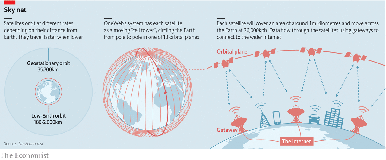
  • OneWeb is a United Kingdom-based company, backed by the UK government and India’s Bharti Enterprises, which is implementing a constellation of LEO satellites.
    • The global communication network powered from space plans to enable connectivity for governments, businesses, and communities.
  • This is OneWeb’s 18th launch (second launch from India) which completed OneWeb’s constellation of 618 low earth orbit satellites that would allow it to offer high-speed, low-latency broadband internet services from space in every corner of the world.
  • The first set of 36 satellites was launched by the LVM3/OneWeb India-1 mission by ISRO on October 23, 2022.
Satellites may connect the entire world to the internet | The Economist

Significance:

  • OneWeb uses a constellation of LEO satellites to provide broadband internet access instead of the traditional method of using satellites placed in geostationary orbits (GEO) 36,000 km above the equator.
  • LEO satellites placed in orbits ranging from 200 km to 1,500 km from earth – compared to 36,000km for GEO satellites – significantly increase bandwidth and reduce latency in space to around 50-70 milliseconds (ms).
    • Latency refers to the time taken by a data packet to be transmitted from a user to the internet service provider through the satellite network.
    • The latency for GEO satellite networks is in the range of 500-700 ms, which limits their use to 2G and 3G communications. 

Project Himshakti

Context: Ministry of Defence has inked a Rs 3,000 crore contract for the procurement of two Integrated Electronic Warfare Systems under Project Himshakti for the Army in mountainous terrain. 

Major Highlights:

  • The contract signed with defence PSU Bharat Electronics (BEL) is under the “Buy Indian-IDMM (indigenously designed, developed and manufactured)” category comprising contemporary and niche technologies. 

Significance:

  • Project Himshakti will generate employment of approximately three lakh man-days over a period of two years. 
  • The project is a significant leap forward in developing indigenous capabilities making the country ‘self-reliant’ in defence manufacturing. 

Semiconductors Manufacturing

Context: The Union Government has disbursed around ₹1,645 crore in performance-linked incentives (PLI) for electronics manufacturers so far, as part of its efforts to bring in more of the electronics supply chain to India. More and more nations are trying to turn away from China’s dominance in the space, following geopolitical pressures to de-leverage themselves from supply chain vulnerabilities.

What are semiconductors?

A semiconductor is a material that allows electrical conductivity between a conductor and an insulator. Semiconductors are made from pure elements like silicon or germanium, or compounds such as gallium arsenide. Sometimes their conductivity is changed through doping.

In a pure semiconductor, such as silicon or germanium, there are few free electrons or holes (missing electrons) available for conduction.

However, when impurities are intentionally introduced into the semiconductor, a process called doping, the number of free electrons or holes can be increased.

They are used to make electronic devices such as transistors, diodes, and integrated circuits (ICs). Transistors, which are used to amplify and switch electronic signals, are made by combining multiple p-n junctions.

Integrated circuits (ICs) are made by creating complex arrangements of transistors and other components on a single piece of semiconductor material. Semiconductors chips are the thumbnail-sized building blocks of almost every modern electronic device from smartphones to connected devices in the Internet of Things (IoT).

Semiconductors have revolutionized the electronics industry and are essential components in nearly all electronic devices, from smartphones to computers to automobiles. Semiconductors make the devices more compact, less expensive, and more powerful.

For instance, mobile phones weighed about 2 lbs, cost around $4,000, and held a charge for only about 30 minutes of talk time during their initial phase. However today an individual can buy a smartphone for 5000 rupees that would give a 1-day charge.

Semiconductor manufacturing in India

The semiconductor chip-making process is complex and highly exact, having multiple steps in the supply chain such as designing software for chips and patenting them through core Intellectual Property (IP) rights. They help give computational power to devices. The global semiconductor industry is currently valued at $500-$600 billion.

The chip-making industry is a highly-concentrated one, with the big players being Taiwan, South Korea and the U.S. among others. In fact, according to a New York Times estimate, 90% of 5nm (nanometre) chips are mass-produced in Taiwan, by the Taiwan Semiconductor Manufacturing Company (TSMC).

Globally, the entire value chain has seeped in the interdependence between a handful of countries like the USA, Taiwan, Japan, China, and some European nations. 

  • India has done well in design and verification for the semiconductor industry. Most of the global semiconductor companies having an R&D footprint in India.
  • However, 100% of our chips, memory, and display are imported into the country, 37% coming from China.
  • Chips import bill is estimated to touch $100 billion by 2025 from $24 billion now. 
  • Although India has two fabs — SITAR, a unit of the Defence Research and Development Organisation (DRDO) in Bengaluru, and a semiconductor laboratory in Chandigarh. These build silicon chips for strategic purposes like defense and space and not for commercial use.

Why is the government encouraging semiconductor manufacturing?

  • National Security: Semiconductors are essential components in many critical industries, including defense, telecommunications, power transmission etc that have implications for national security. Chips made locally will be designated as “trusted sources” and can be used in products ranging from CCTV cameras to 5G equipment. 
  • Strategic competition with China: Countries have spotted strategic value in cornering segments of the value chain for fabs, even as the sophistication and capital needed to run them have climbed to historic highs. China pulled ahead of Taiwan last year, in terms of share of global sales from fabs, according to a report by the Semiconductor Industry Association (SIA).
    • It’s not just India that is wary of this dominance. The U.S. passed the CHIPS Act last August, providing upwards of $280 billion in subsidies and investments to manufacturers opening fabs and making semiconductors in the U.S. This has been combined with restrictions on the Chinese semiconductor industry.
  • Geopolitical Benefits:  driven by data and the digital revolution. Further self-sufficiency will decrease reliance on Chinese chip imports especially during hard times like the recent Galwan Valley border clash.
  • Economic Growth
    • Development of the semiconductor and display ecosystem will have a multiplier effect across different sectors of the economy with deeper integration to the global value chain.
    • Indigenous manufacturing of chips will build its smartphone assembly industry and strengthen its electronics supply chain. 
    • According to the Electronics and IT Ministry, semiconductor demand in India would increase to $70-$80 billion by 2026 with the growing demand for digital devices and electronic products. 
    • This will create numerous employment opportunities for the Indian youth.
    • Indigenous capacity would attract local taxes and boost the export potential. 
    • Further, India would be required to import fewer semiconductor chips which would decrease the import bill.
  • Technological Leadership: Semiconductors are the building blocks of today’s technology. Semiconductor chips are widely used in (a) Computers and laptops; (b) Phones, mobile devices and other electronic gadgets; (c) Automobiles; (d) Aviation; (e) Medical devices especially diagnostics; (f) Military equipment among others.

These semiconductor chips are the drivers for ICT (Information and Communication Technologies). Semiconductors and displays are the foundation of modern electronics driving the next phase of digital transformation under Industry 4.0.

  • Supply Chain Resilience: The COVID-19 pandemic highlighted the vulnerabilities of global supply chains, including those in the semiconductor industry. Governments are encouraging domestic semiconductor manufacturing to increase supply chain resilience and reduce dependence on foreign suppliers. The pandemic and the subsequent lockdowns impacted the supply of chips to India. Automobile manufacturers like Mahindra & Mahindra and Tata group were compelled to reduce their production due to the shortage.
  • Environmental Concerns: The semiconductor manufacturing process can be energy-intensive and can produce hazardous waste. Governments are encouraging domestic semiconductor manufacturing to promote more sustainable and environmentally friendly practices.
  • Changing work and employment pattern 
    • Experts estimate that around 50 crore people will join the internet in the next decade thereby demanding more phones and laptops. 
    • Work from home culture warrants an enhanced demand for servers, internet connectivity, and cloud usage.

Initiatives taken to promote indigenous Semiconductor capacity

  • National Policy on Electronics 2019: It envisions positioning India as a global hub for Electronics System Design and Manufacturing (ESDM) sector. It aims to encourage the development of core components, including chipsets. 
  • Scheme for Promotion of Manufacturing of Electronic Components and Semiconductors (SPECS):
    • The government will provide a financial incentive of 25% on capital expenditure for a list of products that constitute the supply chain of electronic products. This includes products such as electronic components, semiconductors, and specialized sub-assemblies.
    • India would be offering more than $1 billion in cash to each semiconductor company that sets up manufacturing units in the country.
  • Modified Electronics Manufacturing Clusters (EMC 2.0) Scheme: Under this, the government will provide support for the setting up of Electronics Manufacturing Clusters (EMCs) and Common Facility Centres(CFCs).
  • Production Linked Incentive Scheme(PLI): Under this, the government will provide an incentive of 4% to 6% on goods manufactured in India and covered under target segments to eligible companies for a period of five years.
  • Incentive to all nodes of semiconductors: The new changes have been announced to harmonise government incentives for all technology nodes of semiconductors. In the previous version of the scheme, the Centre was offering to fund 30% of the project cost for 45nm to 65nm chip production, 40% for 28nm to 45nm, and 50% or half of the funding for chips 28nm or below. The modified scheme provides uniform 50% fiscal support for all nodes. Besides, it will provide 50% of capital expenditure for other steps of the process as well (chip design and ATMP).
  • Foreign Direct Investment: The Government of India has allowed 100 percent (FDI) under the automatic route in the Electronics Systems Design & Manufacturing sector.  

What are the challenges in front of India?

  • High Cost of establishment: Fabs are highly capital-intensive undertakings, costing billions of dollars for large facilities. As per a government estimate, it would cost roughly $5-$7 billion to set up a chip fabrication unit in India.  
  • Low Ease of doing business: The process of establishing an indigenous semiconductor facility requires clearances and approvals from multiple government departments. 
  • Technological Constraint: The indigenous manufacturing of semiconductors requires the use of high-end technologies. These technologies are licensed from patent holders at a very high price.
  • Lack of Fabrication Capacities: India has a decent chip design talent but it never built up chip fab capacity. The ISRO and the DRDO have their respective fab foundries but they are primarily for their own requirements and are also not as sophisticated as the latest in the world.
  • Structural constraint: FDI in electronics is less than 1% of the total FDI inflow because of the dearth of skilled labor, delays in land acquisition, and the uncertain tax regime.
  • Unstable power supply: The smooth production of semiconductors requires the availability of an uninterrupted 24*7 power supply. they require highly reliable and high-quality supply of water, electricity, and insulation from the elements, reflecting the high degree of precision, cost and capital needed to make the sophisticated circuits.
  • Resource Inefficient Sector: Chip fabs are also very thirsty units requiring millions of litres of clean water, an extremely stable power supply, a lot of land and a highly skilled workforce.

Suggestions

  • Augmenting Research and Development Potential: For instance, IIT Madras developed a microprocessor named ‘Moushik’ with funding support from the Ministry of Electronics and Information Technology.
  • Fiscal Support for All Elements of Chip-Making Chain: Considering India’s considerable talent and experience, it may be best if the new mission focuses fiscal support, at least for now, on other parts of the chip-making chain including design centres, testing facilities, packaging, etc.
  • Establishment of Sovereign Patent Fund (SPF): The proposed Sovereign Patent Fund under National Policy on electronics should be established expeditiously. It is a wholly or partly Government-backed entity that aims to bolster domestic businesses through the acquisition and licensing of patented technology.
  • Push for Quad Supply Chain Resilience Fund: India needs to push for a Quad Supply Chain Resilience Fund to immunise the supply chain from geopolitical and geographic risks.
  • Research ecosystem: government must focus on emerging technologies like LiDAR and Phased Array in which incumbents do not have a disproportionate advantage and the entry barrier is low.
  • Focus on Manufacturers' Assurance of Domestic Procurement – The manufacturers need to be given an assurance of minimum domestic procurement by the government and the private sector. The focus should be on manufacturing economical and technically viable options like 28nm chips.
  • Support for Acquisition of Semiconductor Manufacturing Units: The government should also support businesses in the acquisition of semiconductor manufacturing units in other countries. This is easier than setting up a domestic facility and can be done swiftly for ensuring a continuous supply of chips.
  • Free-Trade Agreement Negotiations: India and Taiwan have started negotiations for a free-trade agreement and setting up a semiconductor manufacturing hub in an Indian city, signalling their resolve to further expand the two-way economic engagement.

Lab Grown Diamonds

Context: Budget 2023-24 has introduced incentives for lab grown diamonds.

About Lab Grown Diamonds (LGDs)

  • Lab grown diamonds (also known as lab created diamonds, manmade diamonds, engineered diamonds, and cultured diamonds) are grown in highly controlled laboratory environments using advanced technological processes that duplicate the conditions under which diamonds naturally develop when they form in the mantle, beneath the Earth’s crust. 
  • These manmade diamonds consist of actual carbon atoms arranged in the characteristic diamond crystal structure. Since they are made of the same material as natural diamonds, they exhibit the same optical and chemical properties.
  • Lab Grown Diamonds is a technologically and innovation driven emerging sector with high employment potential. These environment friendly diamonds which have optically and chemically the same properties as natural diamonds. 

Reasons for interest in Lab Grown Diamonds

  • Mining Free: These diamonds are produced in laboratories. Hence, they are an environmentally responsible choice as a no mining is required.
  • Quality: Lab Grown Diamonds have same physical, chemical and optical properties as mined diamonds.
  • Value for Money & Affordable: Lab grown diamonds offer excellent value. They are more cost-effective than natural diamonds of comparable size and quality.
  • Scarcity of diamonds: As natural diamonds become scarce due to depleting reserves and escalating costs. 
  • Strengthening India’s Gems & Jewellery Industry: India is a global leader in cutting and polishing of natural diamonds, contributing about 3/4th of global turnover by value. With the depletion of natural diamonds, the industry is moving towards Lab Grown Diamonds. 

Process of making Lab-Grown Diamonds

  • Lab Grown diamonds are made in laboratories with a seed of natural diamonds, which is a slice of another diamond - on which the LGD is created. It takes less than month to make a distinctively shaped crystal of Lab Grown Diamond. 
  • There are two methods by which LGDs are created: (i) Chemical Vapour Deposition (CVD) method (ii) High Pressure, High Temperature (HPHT) method.
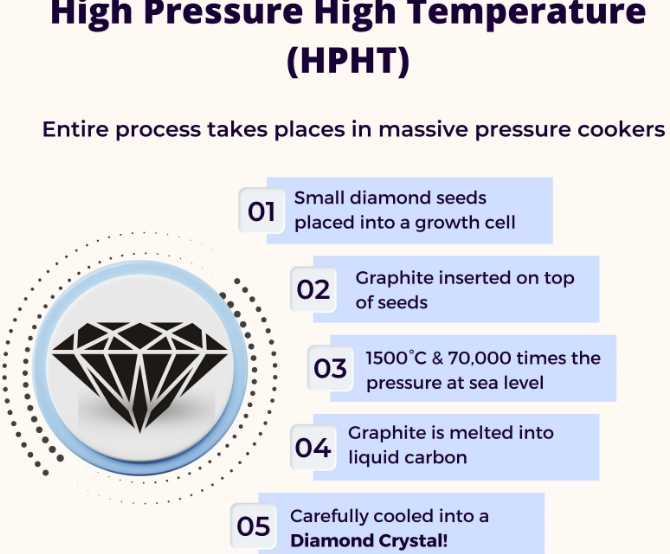
  • High Pressure, High Temperature (HPHT) method: This process mimics the high-pressure, high-temperature conditions that occur under the Earth to form a natural diamond. The seed and graphite carbons are exposed to extreme temperatures (1,500oC) and with extremely high pressures to make LGDs. This method can also enhance the colour of diamonds making them colourless, pink, green, blue or yellow. Diamonds produced by this method may have some impurities of Boron or Nitrogen. This method is popular in China. 
high pressure high temp
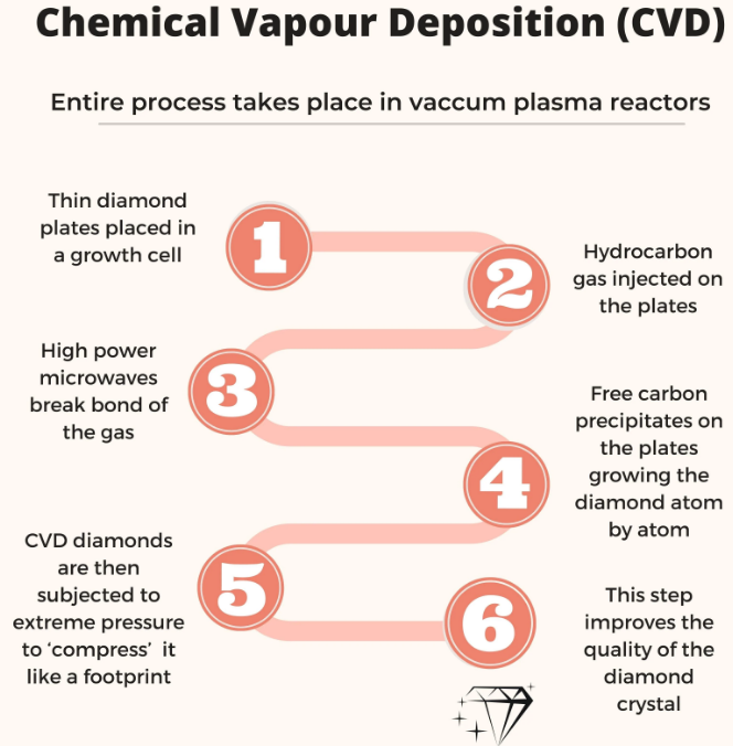
  • Chemical Vapour Deposition (CVD) method: It is a chemical process in which the seed is heated up to 800oC in a sealed chamber filled with molecules of carbon-rich gas such as methane. These gas molecules are broken down into carbon and hydrogen atoms, which get deposited on the seed giving it a shape of square, tabular diamond crystal. This process also requires heat or irradiation to give the crystal a colour effect. Diamonds produced by this method most chemically pure diamonds i.e., free from impurities of nitrogen and boron. CVD method is more popular in India. 
chemical vapour deposition

Identification of Laboratory Grown Diamonds

  • Laboratory grown diamonds require advanced testing in a gemmological laboratory to be identified with certainty. 

Proposals in Union Budget 2023-24 for Lab Grown Diamonds

  • Grant for R&D: To encourage indigenous production of LGD seeds and machines and to reduce import dependency, a R&D grant will be provided to one of the IITs (IIT Madras) for five years.
  • Relief in Customs duty: Budget 2023-24 has abolished customs duty on imports of seeds used for manufacturing of rough lab-grown diamonds. This will boost domestic manufacturing of LGDs and reduce imports of LGDs. 
  • Implications of Fiscal support: Fiscal support provided for LGDs is aimed at boosting exports of LGDs from India and to reduce dependence of imports for key inputs i.e., seeds and equipments. 
  • LGDs in India: In India, share of LGDs in overall diamond business is just 2-3% with LGDs being used majorly for jewelleries and exports. About 80% of cut and polished LGDs are exported, while only 20% are consumed globally. 
  • Trends in LGD trade: India imported rough LGDs worth Rs 7,656 crore in April-December 2022 and exported 10,587 crores of LGDs in the same period. US & Europe are key markets for India’s CVD labs grown diamonds. With further government support, LGD industry will become competitive globally. 

Diamond Simulants

  • Diamond stimulants, such as cubic zirconia and moissanite, look like diamonds but are not true carbon crystals. Simulants do not have the same chemical and physical properties as natural diamonds and therefore sell at much lower prices than lab created diamonds. 
  • Moissanite is a gemstone born from stars and was first discovered in a crater created by a meteorite in Arizona, USA. They are composed of crystal of silicon carbide and not of carbon as diamonds. However, they appear like Diamonds. 
  • Natural Moissanite is incredibly rare on Earth. Hence, most moissanite available today is laboratory created. Moissanite, referred to as a diamond simulant, is engineered to give the illusion of similarity to diamonds, but is compositionally and visually quite different from a real diamond.